Samsung Electronics has now announced that it has begun mass production of its 236-layer 3D NAND flash memory chips, which the company has named the 8th generation V-NAND.
The new generation of memory chips can bring a transfer speed of 2400MTps. When used with a high-end controller, it can easily make the transfer speed of consumer SSDs exceed 12GBps.
Join us on Telegram
According to reports, the 8th generation V-NAND can provide a 1Tb solution. Samsung Electronics has not disclosed the size and actual density of the IC, but they call it the highest bit density in the industry.
Samsung claims that its next-generation 3D NAND flash can improve mono productivity by 20% compared to existing flash chips of the same capacity, further reducing costs (at the same yield), which may mean that everyone can expect to buy a cheaper solid-state drive of the same capacity.
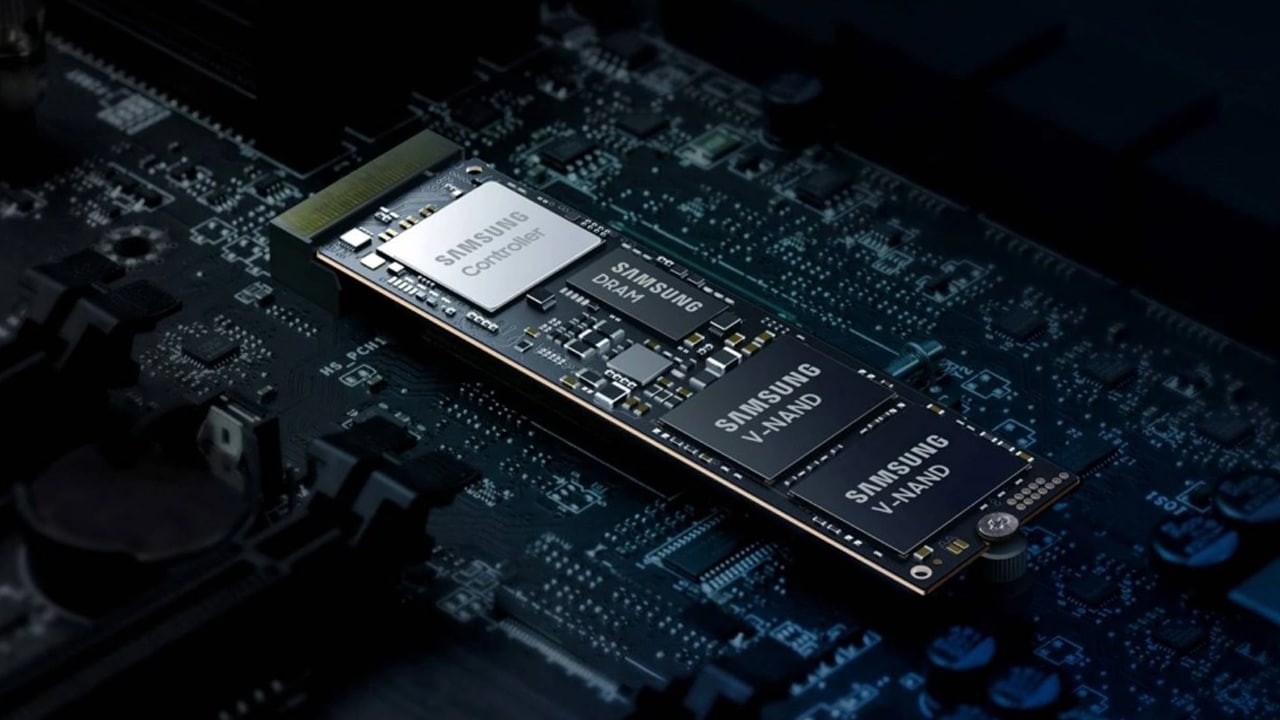
The company didn’t reveal the new architecture, but based on the images provided, we can assume it’s a dual-plane 3D NAND chip.
 SungHoi Hur, executive vice president of flash memory products and technology at Samsung Electronics, said: “As the market demand for denser, higher-capacity storage drives higher V-NAND layer counts, Samsung employs advanced 3D compression technology to reduce surface area and height while avoiding the cell-to-cell interference that typically occurs during compression.”
“Our 8th generation V-NAND will help meet rapidly growing market demands and allow us to better offer more differentiated products and solutions. , which will be the foundation of future storage innovations.”
In the middle of this year, Samsung launched its eighth and ninth-generation V-NAND products and fifth-generation DRAM products. Prior to this, the company currently offers 512 Gb triple-level cell (TLC) products for V-NAND.
In addition, fifth-generation DRAM products will be 10nm (1b) devices that will enter mass production in 2023. Other upcoming DRAM solutions from Samsung include 32 Gb DDR5 solutions, 8.5 Gbps LPDDR5X DRAM, and 36 Gbps GDDR7 DRAM.
Samsung claims for its V-NAND that by 2030 it will have 1000 layers of V-NAND. To achieve this, Samsung is transitioning from its current TLC architecture to a quad-level cell (QLC) architecture to increase density and enable more layers.
Moreover, Samsung will also invest more resources in DRAM R&D, researching new architectures and materials, such as High-K, to help expand DRAM beyond 10nm. The company intends to further develop other DRAM solutions, such as in-memory processing (PIM).